Haotong Liang
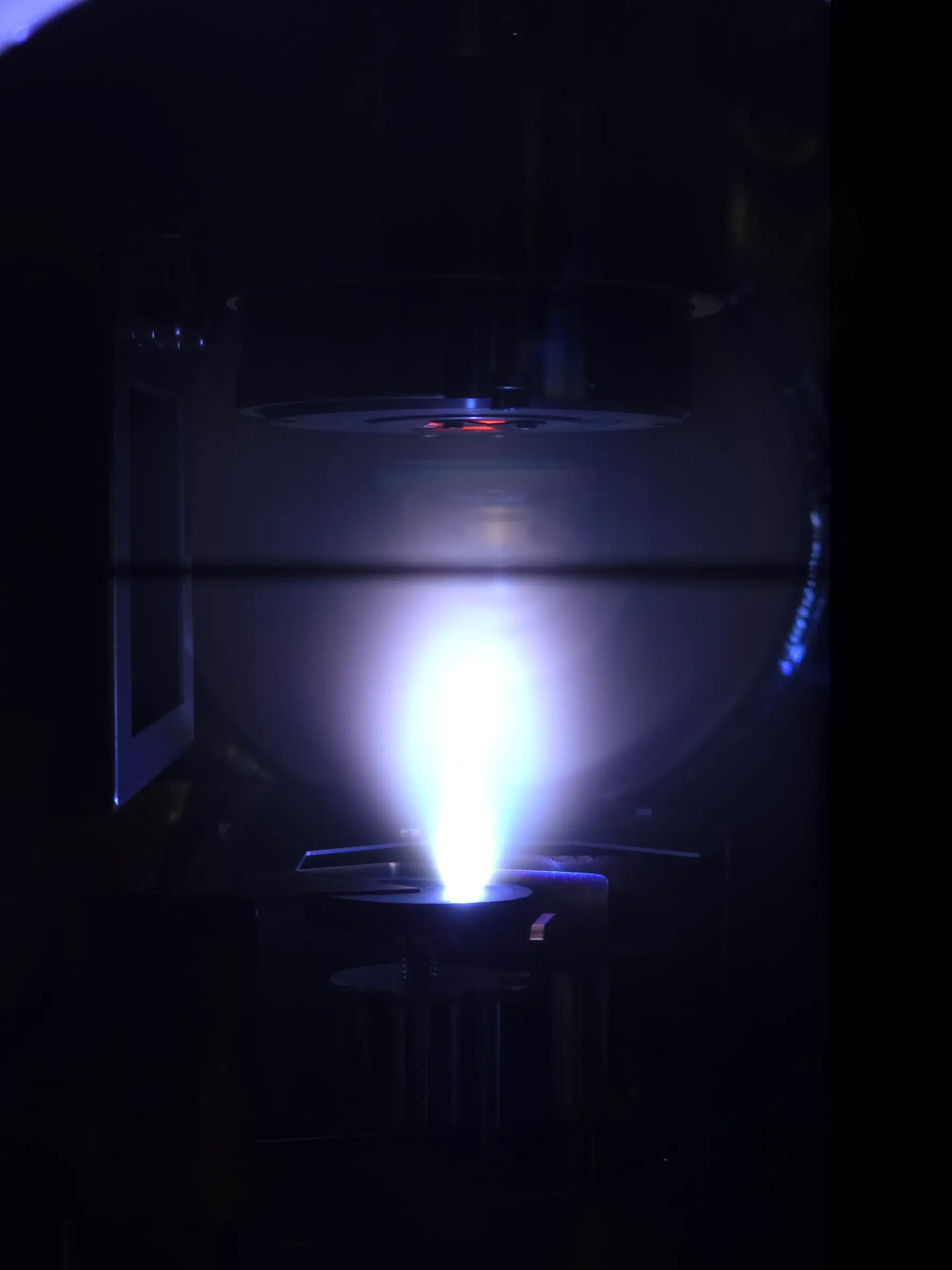
A pulsed-laser ablation plume crossing a deposition chamber

Ph.D., Materials Science & Engineering · University of Maryland · August 2026

I build laboratories
that run themselves.

Deep learning and Bayesian inference, wired directly into deposition chambers, diffractometers, and additive-manufacturing machines — so the experiment can decide what to do next while it is still running. Here is what that looks like.

7publications, 4 as first author
Science Advancesfirst author, 2025
8 yearsin the Takeuchi group
100×the throughput goal
01

The self-driving thin-film lab

Pulsed-laser deposition with a computer-vision loop closed around it. The instrument decides what to grow next while the growth is still happening.

The self-driving thin-film labPLD chamber, RHEED optics, and the control stack that runs them without me in the room.
Ablation plumeA pulsed laser hits the target and a few atomic layers cross the chamber.
RHEED, streak by streakA well-etched, well-annealed substrate read live by the segmentation model.
PLD system, other sideVacuum, gas handling, and laser optics all have to agree before anything grows.
Heater block diagnosticChasing a few degrees of non-uniformity across the sample stage.
Aligning the pyrometerThrough the viewport, onto a substrate already glowing.
Troubleshooting the electron sourceThe hairpin tungsten filament that supplies electrons to the RHEED gun by thermionic emission. Arcing across its metal contacts had burned it out early.
Wehnelt cap assemblyThe small part that decides whether you get a usable electron beam.
A PLD targetEvery film starts as a pressed and sintered puck like this one.
Laser spot calibration couponBurn patterns that tell you where the beam actually is.
Selective deposition designMasked geometry that puts several growth conditions on a single substrate.
Substrate annealingA high-temperature soak to pull an etched surface back into atomic terraces.
Sputtering plasmaArgon glow discharge, mid-deposition.
CathodoluminescenceAn Al₂O₃ substrate lighting up under the electron beam.
02

Machine learning

The models behind the loop: instance segmentation that reads diffraction patterns as they arrive, peak fitting that turns them into numbers, and Gaussian-process Bayesian optimization deciding what to measure next.

RHEED, segmented and classifiedInstance segmentation separates the direct beam, the streaks and the spots, each with its own confidence; a second head calls the growth mode.
Peak detection and fittingSmooth, detect, then fit — separating overlapping peaks from the background is what turns a raw pattern into numbers a model can use.
The optimizer, thinkingGaussian-process posterior and UCB acquisition over fifteen iterations — the loop that picks which experiment to run next.
A phase diagram, built autonomouslyBayesian optimization with a CALPHAD prior chose every measurement. The thin-film Bi–Sn eutectic lands near 133 °C, below the bulk 141 °C.
03

The stack, in the open

The software that runs the self-driving lab is public. Both halves of it — the control stack and the console — MIT-licensed on GitHub.

Lumi-Deck, the operator consoleLive diffraction video, model inference, and intensity tracking in one browser tab. Open source.
The control stackInstrument control, the RHEED camera and the ML node all speak through one message queue, with a React front end and an API on top of it. This is the architecture of Lumi-Lab and Lumi-Deck.
04

Reading structure

Diffraction, microscopy, and microprobe work — the measurements that tell you whether the thing you made is the thing you meant to make.

My first pole figureTexture in a thin film, resolved for the first time.
Composition-spread libraryOne wafer, hundreds of compositions, measured point by point.
Full-circle diffractometerFour-circle goniometry for texture and pole-figure work.
AFM defect mappingSurface topography of an epitaxial film, hunting for what went wrong.
Library on the goniometerAligned and ready for a long automated scan.
In-situ phase mapping, Sn–BiComposition and temperature swept together, diffraction running throughout.
High-speed powder diffractionSix detector frames stitched into one strip; the boxed region is what gets integrated into a pattern.
WDS microprobeWavelength-dispersive spectroscopy when EDS is not quantitative enough.
Calibrating deposition rateStylus profilometry across a masked step turns laser pulses into ångströms.
05

Beamtime

Hardware I built, shipped to SSRL at SLAC, and ran around the clock. Synchrotron time is allocated in shifts, and nothing gets a second take.

Flash-annealing rig at beamline 17-2Built for real-time diffraction during rapid thermal processing at SSRL.
The rig, close upLamp heating, gas handling, and the X-ray path inside a 30 cm envelope.
2D GIXRD, liveDiffraction arcs arriving on the detector while the sample is still heating.
Beam damageWhat a synchrotron leaves behind when the exposure runs too long.
BeamtimeThe hutch at SSRL — beamtime is measured in shifts, not hours.
06

Metal, melted

Bayesian optimization applied to laser powder direct energy deposition, with in-situ X-ray imaging built to see the melt pool as it forms.

As-built LPDED wall — crackedLaser powder direct energy deposition of a Ni superalloy; the process window shows itself in the cracks.
As-built wall — wavy topLayer-height drift accumulating over a build, and an objective worth optimizing against.
The crack, up closeSEM cross-section of the etched alloy. Thermal stress opened this one straight through the columnar grains.
In-situ X-ray imaging, installedWatching the melt pool while the laser is still running.
Getting control of a commercial machineA TruLaser Cell 3000 that never shipped with an API, wired for programmatic control.
The same system, on the benchSource, detector, and motion control breadboarded before anything went into the machine.
Polished Ni superalloyMounted and mirror-finished for microstructure work.
Two coupons on the stageSame alloy, different build parameters.
The sample archiveEvery build gets bagged, labelled, and kept.
Laser-cut partsCustom fixtures, cut in-house, for a one-off experiment.
What is left of the plateThe negative space of a batch of samples.
07

The fab floor

Dicing, lithography, evaporation, milling. Automation only earns its keep if the sample preparation underneath it is sound.

Dicing sawCleanroom wafer dicing, one street at a time.
A diced libraryA gradient wafer cut into individually addressable chips.
Dicing in progressBlade, coolant, and a very slow feed rate.
Spin coaterResist going down at three thousand revolutions per minute.
Evaporated gold contactsShadow-masked pads for transport measurements.
The resist benchPhotolithography chemistry, waiting its turn.
Ion millLoading a sample for surface cleaning before deposition.
Milled samples on the platterOut of the mill, clean and ready.
08

Passing it on

Autonomous experimentation should not require a synchrotron to learn. Legolas is the cheap, teachable version of the same loop.

LegolasA low-cost closed-loop experimentation platform built to teach autonomous science.

The written version

Everything above, in one page of text.

Publications, methods, coursework, and the full research history — formatted to read and to print.

Open résumé